
Are you puzzled by the concept of the Zener Diode? Looking for a reliable platform to understand it easily? Don’t worry, you’re absolutely in the right article!
Today In this article, we are going to explore everything about Zener Diode. We’ll focus on some key areas such as, what a Zener diode is, some prerequisites to understand the topic, its classification, diagrams, and a few more extra concepts to strengthen the understanding.
By the end of this article, you’ll have a complete understanding of Zener diode. So, let’s get started! But before diving into the Zener diode itself, we have to understand some of it’s pre-requisites first, so let’s start..
What is Semiconductor?
A Semiconductor is a material whose electrical conduction is due to the movement of electrons in the conduction band and the movement of holes in the valence band. Its electrical conductivity lies between a conductor and an insulator.
Semiconductors are classified into two types:
1. Intrinsic Semiconductor:
A pure semiconductor which is free of every impurity is called intrinsic semiconductor. The electrical conductivity of a pure semiconductor is completely controlled by electrons. For example: Silicon (Si) and Germanium (Ge).
2. Extrinsic Semiconductor:
A doped semiconductor or a semiconductor with suitable impurity atoms added to it, is called extrinsic semiconductor.
Extrinsic semiconductors are further classified into two types:
1. N-type Semiconductor:
When a pure semiconductor of silicon (Si), is doped with a controlled amount of pentavalent atoms. For example: arsenic, phosphorus, antimony or bismuth, is called n-type semiconductors.
2. P-type Semiconductor:
When a pure semiconductor of germanium (Ge), is doped with controlled amount of trivalent atoms. For example: gallium (Ga), indium (In), boron (B) or aluminium (Al), is called p-type semiconductors.
What is Doping?
Doping is a process of adding desirable impurity atoms to a pure semiconductor. The impurity, atoms added are called dopants.
What is P-N Junction?
When a p-type semiconductor is brought into close contact with n-type semiconductor crystal, the resulting arrangment is called p-n Junction diode.
There are two methods of biasing in the P-N Junction:
1. Forward Biasing:

A p-n junction is said to be forward biased if the positive terminal of the external battery is connected to p-side and the negative terminal to the n-side of p-n junction.
2. Reverse Biasing:
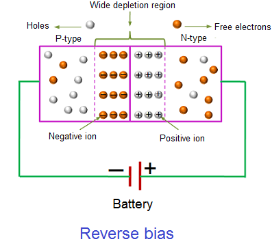
A p-n junction is said to be reverse biased if the positive terminal of the external battery is connected to n-side and the negative terminal to p-side of the p-n junction.
Characteristics of a P-N Junction Diode:
1. Forward Voltage Drop:
A small voltage across a conducting diode, is called the forward voltage drop and is about 0.7 V for normal diodes which are made from Silicon. The forward voltage drop of a diode is almost constant whatever the current passing through the diode so they have a very steep characteristic.
2. Reverse Voltage:
When a reverse voltage is applied a perfect diode does not conduct, but all real diodes leak a very tiny current. This can be ignored in most circuits because it will be very much smaller than the current flowing in the forward direction. However, all diodes have a maximum reverse voltage (usually 50V or more) and if this is exceeded the diode will fail and pass a large current in the reverse direction, this is called breakdown.
3. Rectifier Diodes:
Rectifier diodes are used in power supplies to convert alternating current (AC) to direct current (DC), a process called rectification. All rectifier diodes are made from silicon and therefore have a forward voltage drop of 0.7V.
There are two types of characteristics of a p-n junction diode:
1. Forward Characteristics:
This gives, how diode behaves, when the positive terminal of a voltage source is connected to the P-type side and the negative terminal to the N-type side. This causes the depletion region to narrow, because majority charge carriers attracted towards the junction. When the voltage is low, small current flows. At threshold voltage or knee voltage current starts to increase rapidly. Threshold voltage for Silicon diodes is around 0.7V and for Germanium around 0.3V. After threshold voltage current increases exponentially with voltage.
2. Reverse Characteristics:
This gives, how diode behaves , when the positive terminal of a voltage source is connected to the n-side and the negative terminal to the p- side. This increases the width of the depletion region, because of majority charge carriers are attracted away from the junction, which blocks current to flow. Small reverse saturation current, flow due to the presence of minority carriers. At breakdown, the diode’s resistance drops sharply, and a large current flow, resulting in damage to the diode.
The Zener Effect:
In the presence of sufficient reverse voltage, a p-n junction experiences rapid avalanche breakdown and conducts current in the reverse direction. Under the influence of an applied electric field the free valence electrons can be accelerated so much that they can free other electrons and the subsequent collision quickly become an avalanche. When this process is taking place, very small changes in voltage can cause very large changes in current. The breakdown process depends upon the applied electric field, so by changing the thickness of the layer to which the voltage is applied, zener diodes can be formed which break down at voltages from about 4 volts to several 100 volts.
What is Zener Diode?
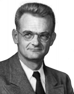
The Zener effect was discovered by Clarence Melvin Zener. With details of electrical characteristics of diode and Zener effect.In which current flows in the opposite direction due to electron tunneling in the heavily doped p-n junction.
The zener diode uses a p-n junction in reverse bias to make use of the zener effect which is a breakdown phenomenon which holds the voltage close to a constant value called the zener voltage. The basic principle of diodes is that they allow current to flow in one direction. When the direction is reversed (reverse bias) the diode does not allow any current to flow in the circuit. This also applies to zener diode as it does not allow current to flow in reverse bias, the zener diode will work like a standard diode.

Zener diodes have a specified reverse breakdown voltage known as the Zener voltage. In reverse bias, the Zener diode prevents current from flowing through the circuit only up to a certain voltage. If the breakdown voltage of the zener diode is 10V and the supply voltage is 5V. In this condition, current will not flow in the circuit. However, when the circuit voltage rises above the Zener diode breakdown voltage i.e. above 10 volts, current will start flowing in the circuit due to increased Zener diode breakdown voltage.
“You may be wondering, what is the advantage of a diode that can conduct current in both directions?”
So here are the all applications, which can answer above question:
- Zener diode as a Voltage Regulator: The zener diode is used as a Shunt voltage regulator for regulating voltage across small loads.
- Zener diode in clipping circuits: Zener diode is used for modifying AC waveform clipping circuits by limiting the parts of either one or both the half cycles of an AC waveform
- Zener diode in clipping circuits: Zener diode is used for modifying AC waveform clipping circuits by limiting the parts of either one or both the half cycles of an AC waveform.
What are Zener and Avalanche Breakdown?

Zener Breakdown:
In highly doped diodes, the depletion region becomes narrow. This high electric field causes the electrons to pass through the depletion region even at relatively low reverse voltage, which leads to zener breakdown. The breakdown voltage decreases with increasing temperature.
Avalanche Breakdown:
In lightly doped diodes the depletion region is wide. The strong electric field at higher reverse voltage accelerates the free electrons, which result in collisions with atoms, creating many new electron-hole pairs. These electron-hole pairs contribute to a significant increase in the current, which leads to avalanche breakdown. The breakdown voltage increases with increasing temperature.
I hope by now all your doubts related to Zener diode have been cleared. If you still have any doubts on this topic or you want me to come up with more articles on semiconductor devices then please, please drop your question in the comment section, I will try my best to answer all your doubts.
“So stay connected, keep smiling!”